|
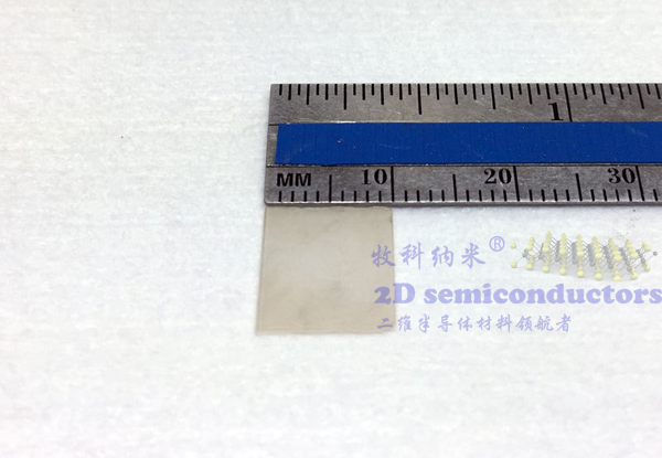
样品照片: 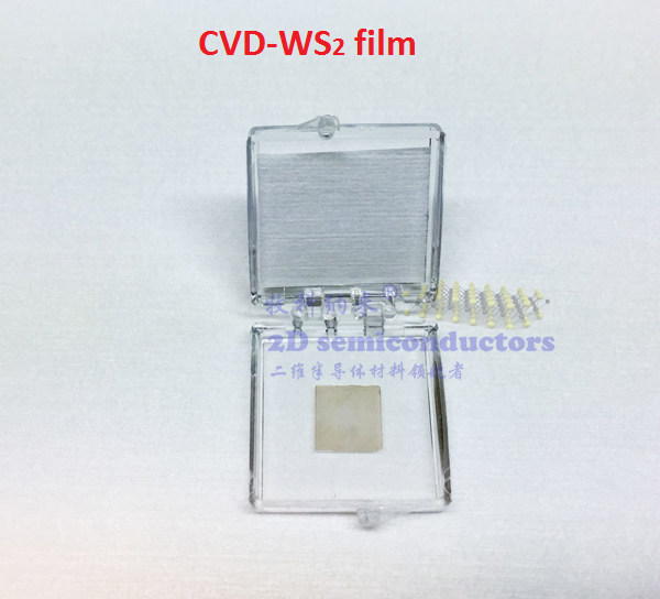
HRTEM: 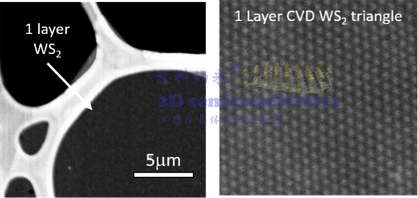
EDX: 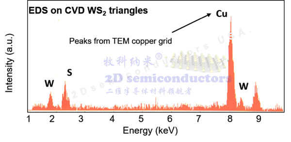
Raman和PL光谱: 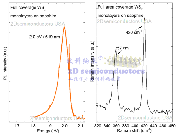
Description: Isolated monolayer thickness WS2 are grown onto c-cut (0001) sapphire substrates. This particular product contains monolayer thickness WS2 triangular flakes randomly distributed across sapphire substrate. While some regions reach continuity with coalesced WS2 triangles, this sample contains well-separated triangles for advanced spectroscopy, microscopy, and electronic measurements. Synthesized monolayer WS2 triangles are highly luminescent and Raman spectroscopy studies also confirm the monolayer thickness. Growth method: Our company synthesizes these monolayers using chemical vapor deposition (CVD) using highest purity (6N) gases and precursors in semiconductor grade facilities to produce crystalline and large domain size samples (1-50um). This is unlike commonly used MOCVD process wherein defects are very very large and domain sizes are small (10nm-500nm). Our samples are always highly luminescent and highly crystallized Sample Properties | Sample size | 1cm x 1cm square shaped | | Substrate type | (0001) c-cut sapphire | | Coverage | Isolated and partially merged monolayer triangles | | Electrical properties | 2.0 eV Direct Bandgap Semiconductor | | Crystal structure | Hexagonal Phase | | Unit cell parameters | a = b = 0.312 nm, c = 1.230 nm, α = β = 90, γ = 120° | | Production method | Low pressure Chemical Vapor Deposition (LPCVD) | | Characterization methods | Raman, photoluminescence, TEM, EDS |
Specification. - Identification. Well-separated WS2 domains across c-cut sapphire
- Physical dimensions. one centimeter in size. Larger sizes up to 2-inch wafer-scale available upon requests.
- Smoothness. Atomically smooth surface with roughness < 0.2 nm.
- Uniformity. Highly uniform surface morphology. WS2 triangles are scattered across sample
- Purity. 99.9995% purity as determined by nano-SIMS measurements
- Reliability. Repeatable Raman and photoluminescence response
- Crystallinity. High crystalline quality, Raman response, and photoluminescence emission comparable to single crystalline monolayer flakes.
- Substrate. c-cut Sapphire but our research and development team can transfer WS2 triangles onto variety of substrates including PET, quartz, and SiO2/Si without significant compromising of material quality.
- Support. 2Dsemiconductors USA is an American owned, regulated, and operated company. Our customers are well-protected by international as well as strict American customer laws and regulations. We give full technical support and guarantee your satisfaction with our well-established customer
- Defect profile. WS2 monolayer triangles do not contain intentional dopants or defects. However, our technical staff can produce defected WS2 using a-bombardment technique.
|