|
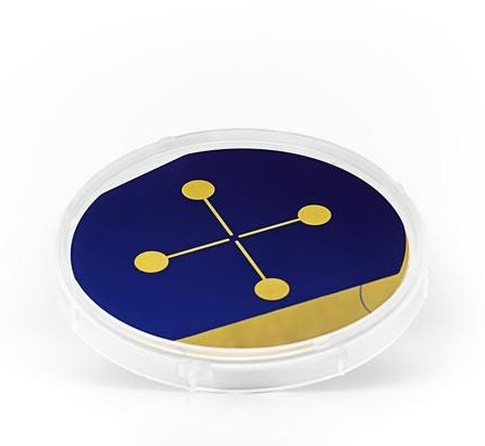
样品数据: 客户提供衬底 
石墨烯样品扫描电子显微镜照片: 
拉曼光谱图: 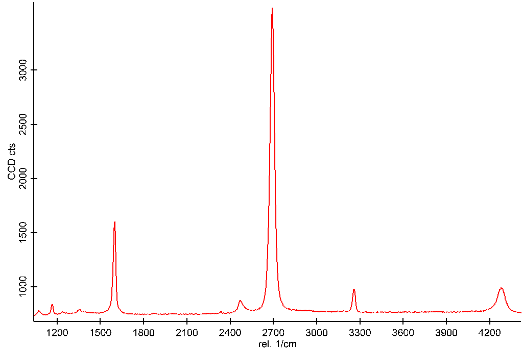
透射电子显微镜照片: 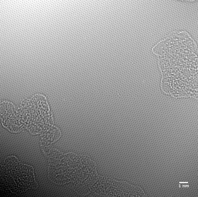
衬底和样品信息: Graphene on Your Substrate - Processed in Clean Room Class 1000 This is a tailor made graphene product. You send your substrate to our laboratory (including your order ID and your email address as a reference) and we then use our innovative method to transfer the graphene monolayer on top of it and send it to the address you specify. Examples of substrates we have successfully transferred graphene to: devices, solar cells, LEDs, gold, alumina, silver mirrors and sapphire. Errors and sapphire. GRAPHENE FILM - · Growth Method: CVD synthesis
- · Transfer Method: Wet transfer method
- · Appearance (Color): Transparent
- · Transparency >97%
- · Appearance (Form): Film
- · Coverage >95%
- · Number of graphene layers: 1
- · Thickness (theoretical) 0.345 nm
- · FET mobility on Al?O?: 2800 cm2/Vs
- · Hall mobility on SiO?/Si: 2000-3500 cm2/Vs
- · Sheet Resistance on SiO2/Si: 450±40 Ohms/sq (1cm x1cm)
- · Grain size: Up to 10 μm
QUALITY CONTROL All our samples are subjected to a rigorous QC in order to ensure a high quality and reproducibility of the graphene. - · Raman Spectroscopy: I(G)/I(2D)<0.5; I(D)/I(G)<0.05
- · Optical Microscopy inspection of each individual sample to ensure good transfer quality and purity
If your application requires more specific controls (AFM, SEM...) please do not hesitate to contact us.
|