|
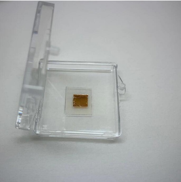
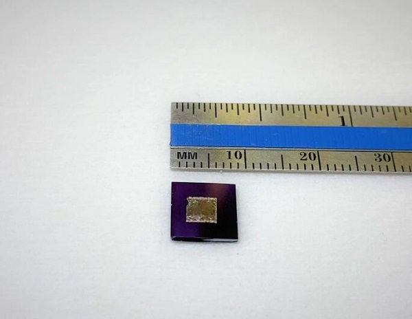
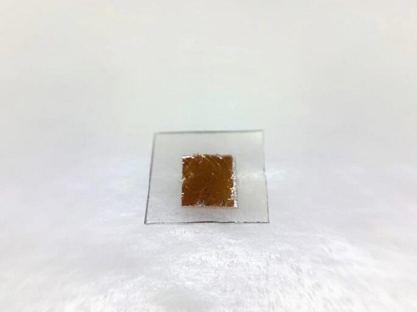
样品照片: 
Raman: 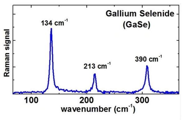
PL: 
样品信息: 
Description: Multilayer gallium selenide (GaSe) films have been synthesized through atomic layer deposition (ALD) growth to enable large single domain thin films with negligible amount of grain boundaries. GaSe thin films are directly deposited onto double side polished c-cut sapphire substrates but can be transferred onto virtually any substrate choice. GaSe films measure 100s of nanometers in thickness and particularly ideal for thin film geometry measurements such as catalysis, photovoltaics, electronic transport, and others. GaSe films come with guaranteed PL, Raman, and semiconducting response.
|